Prototype Styles
Almost every one of these could be built as a final working unit.
UGLY#
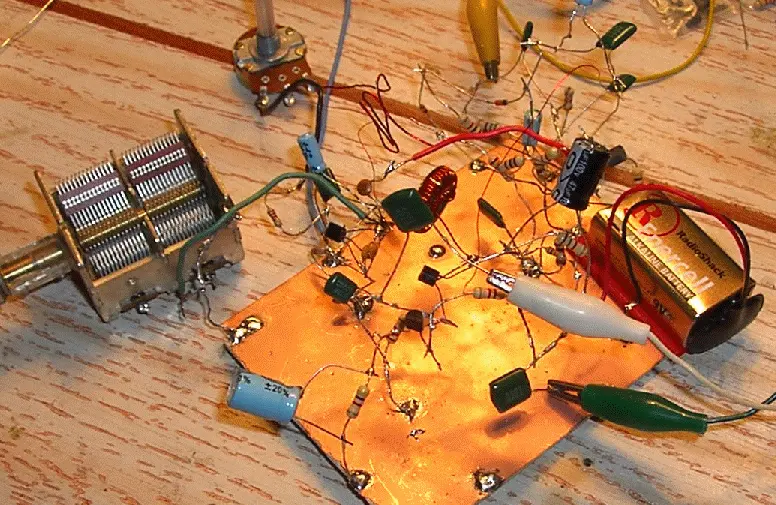
Sometimes ugly circuits are not the prettiest designs. The main reason people use this method is because it's easy to change things quickly.
- There are several explanations for what qualifies as an ugly circuit, but one commonality across all of them is that ugly circuits have contacts that are not completely mechanically coupled to the substrate. But this is not a legal requirement.
- The substrate is usually copper clad, but it isn't always. This method can be difficult to master, as it requires complete balance. A single copper clad board as a giant, unobstructed ground plane is the preferred method that we see being used. Passive components, such as resistors and capacitors, are usually the easiest to start with.
- It's a good starting place to solder one side to ground, then solder the other side to another component. This can be a great benefit to radio frequency circuitry or any circuit that requires a solid ground. An unobstructed copper clad board ensures a strong connection to ground.
Notable persons with a PhD dislike using Ugly style build methods. These types of people are highly qualified, but may lack common sense.
This is another Ugly RF construction that is mostly floating in the air and is not so robust. However, it is quick with this method to change out Components, adjust the Circuit for any number of reasons.
The Ugly method is the least likely style for making a final circuit that will serve over many years.
NO SUBSTRATE#
An Arduino Uno that was not made using a substrate, but simply wires and components. Kimo Kosaka made it, but it's not at all ugly. However, it uses the ugly style of construction.
Circuits that are considered to be unattractive, or ugly, do not necessarily have to have a substrate, but it does not make the process of building such a circuit any easier. There are many examples out there of circuitry that is made simply by connecting pins to pins with small wires. It can be very difficult to make a circuit like this, but it is a valid art form.
The wires that connect the parts together can be part of the structure of the unit and, if done correctly, could be strong. It can be built with just a soldering iron and solder if you have the components, as the construction method can be useful in certain circumstances. Even though some circuits made with this method are very beautiful, most are called Ugly, even though they are art forms.
DEAD BUG#
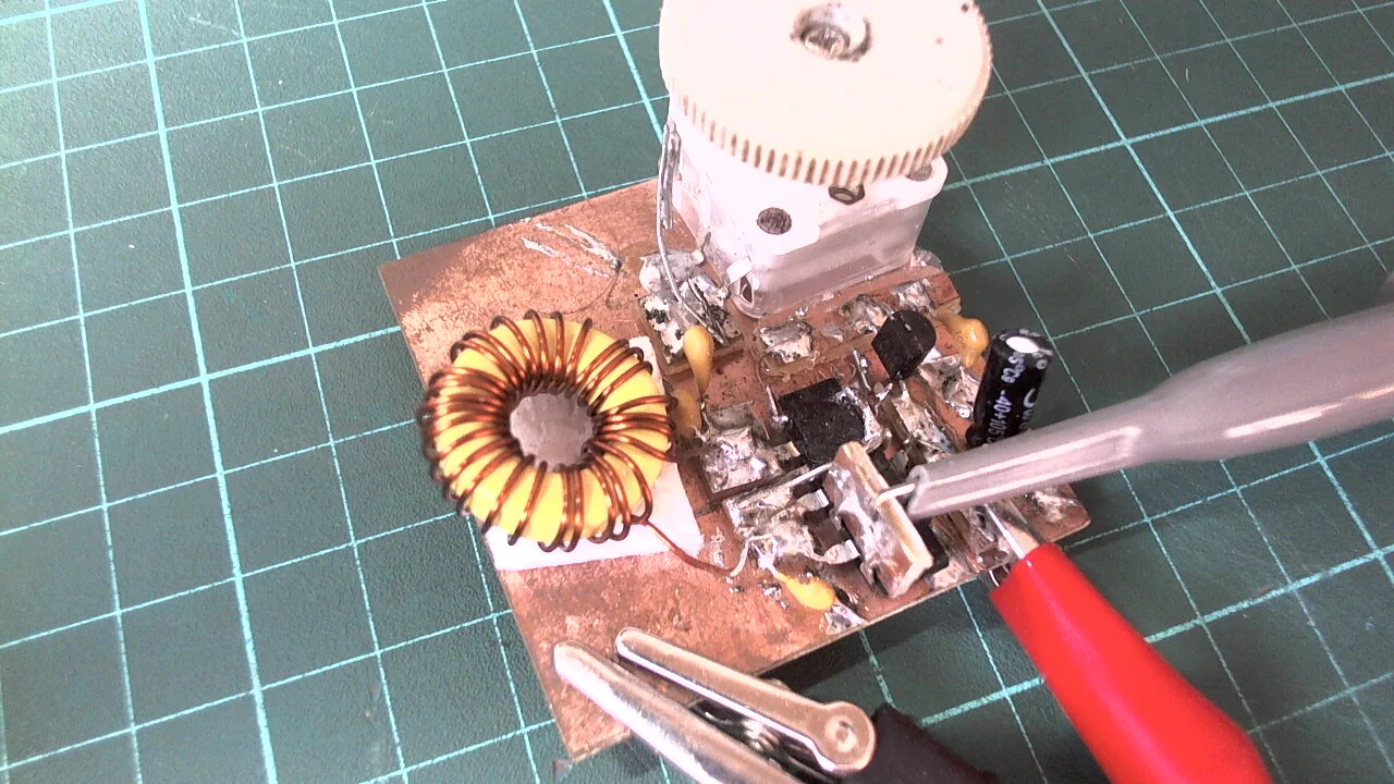
This is a Messy Manhattan/ Dead Bug circuit - it is an RF Oscillator, made by Geoff of YOOFAB and it works really well.
The idea is to take an IC, traditionally in a DIP package, and set it upside down on the copper substrate. Usually glueing the IC to the copper is best, but this is not always necessary.
With the pins facing upwards, it looks like a dead bug.
If required, the pins can be bent to face the substrate, but they typically face upwards. The pins are connected directly to passive components leads or wires to other chips, taking many methods from the ugly style.
This implies the connections are in the air. The benefit to this method is that you don’t have to waste time drilling holes in the substrate, and can integrate IC’s into an ugly design fairly easily.
When using this method, be aware that the pins on the chip will be flipped when placed upside down. To figure out pin-numbers is more difficult than to make a layout-diagram.
DEAD BUG MODIFIED#
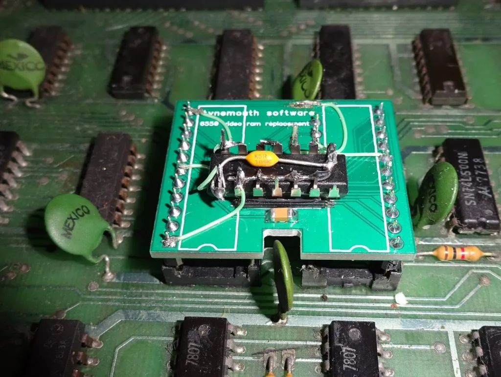
This is an example of a modification to a PCB that has been done Dead Bug style to make the thing work, while waiting for the real part to arrive.
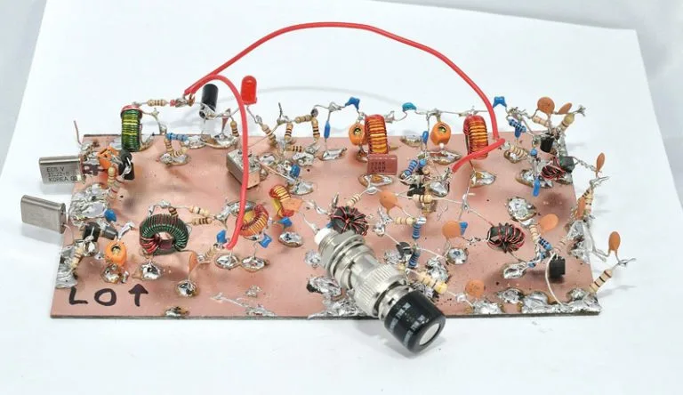
MANHATTAN STYLE#
Manhattan style is named after the Manhattan borough of New York City, which is known for its skyscrapers.
- Manhattan style uses cut out sections of copper board as islands. This method means there are no connections floating in the air. All points on a component are connected to copper in some way.
- This often results in a board that is laid out in a much clearer way, which is easier to follow and replicate. It also allows for the use of surface-mount components, which is practicable, but extremely difficult with ugly.
- The small pads don't have to be separate from the larger ones. The process would be cheaper if they were cut out of the backplane. However, you should be aware that there is a possibility that you will make a mistake and damage the board. You can, of course, cut into the copper substrate to create the islands, but this is a permanent process and is difficult to reverse.
- Manhattan can be a quick and easy method of construction. Another possible reason for the name Manhattan is that the capacitors and resistors tend to line up and are perpendicular to the substrate. The substrate is usually copper and this forms the ground plane.
CRITICISM#
- It is true that small copper pads will produce Capacitance. The larger the pad and the thinner the PCB material, the higher the capacitance will be. You may be better off making your own pads than buying the extremely thin types available from QRPme. If you don't live in Yankside, this is true. In reality any method of cutting non FR4 material is fine.
- However, respect is due to Rex W1REX for his contributions to the Manhattan Build Methodology, which is now accepted as a standard.
- A 1 cm square pad with a PCB thickness of 1.5 mm will be around 4 pf. This may seem like a trivial matter, but in some applications, especially at VHF frequencies, this capacitance can be a critical factor. It can also really mess up your whole circuit, as the capacitance can add up across the board.
DIRECT TO PCB WITH NO TESTING#
Another way to do things is to Go-Direct to any of the www.ChongPongWingDongPCBDirect.com sites. Under this modality, you do not bother prototyping at all. Rather you pass this step and go directly to the PCB manufacturing house.
This way, it costs you something like $5 for 5 PCBs. However, you have no idea of the validity of your Design nor your Layout. This may result in boxes of boards are of NO use whatsoever; all because you missed the whole point of Prototyping.