The Law of Electronics
THE LAW OF ELECTRONICS IS ABSOLUTE AND FINAL!#
- These laws are absolutely unbreakable.
- If you do that, you will be in serious trouble.
- The Barefoot Methodology follows these laws.
- The law must prevail, and much danger may result from violating it, so those who violate it must be ridiculed immediately.
- It is an offence to be unfamiliar with electronic law.
- There are no excuses.
- The electronic law is based on scientific findings and methods.'
- Until new rulings or a paradigm shift in physics occur, these laws are an axiom.
- Electronic law is not boring, it is exciting.
- Obeying the law will make circuits behave well.
- If you don't obey, the circuit won't obey either, so things will be unpredictable.
Current flow
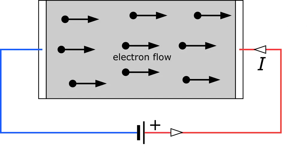
THE CONVENTION OF CURRENT FLOWING FROM POSITIVE TO NEGATIVE.#
This picture falsely illustrates current flow in a conductor. It is important to note that the electrons move from negative to positive. However, it is customary to consider current to flow from positive to negative. You don't need to worry about it. It's just a rule that everyone follows.
-
Current is a flow of electric charge. The charge is a flow of electrons, moving through a wire or circuit path. It is measured in amperes (A) and this flow has a direction.
-
The convention is that Current flows from positive to negative. However, in reality electrons carry a negative charge, and so it is that the flow of electron charge is from Negative to Positive.
- We do not get Vexed, nor Worked-up over this, it is just a convention and in terms of energy flow, it makes total sense if you think of this as a flow of positive charges.
- If you become very Distressed, Vexed and Worked-up over this issue, you are advised to listen to: In green tea, great wisdom is found.
-
A Current source of five amperes transports five Coulomb(s) of charge per second.
VOLTAGE LAW#
-
Electrons can have Electric Potential Energy.
-
An Electron situated at the ground node has zero Potential Energy.
-
The Energy Level Changes as it travels between circuit nodes.
-
The voltage difference (V) between two nodes is the amount of Energy Charge that is gained or lost as Current transfers from one node to the other.
-
So, here we might see the Voltage as if it were the height from the ground.
-
We display voltage differences between the ground and all nodes.
-
The ground node provides a reference for all nodal voltages.
-
The voltage source on a Schematic Diagram is an electronic component that upholds a specified voltage difference across its terminals, independent of the Current passing though it.
-
A one Coulomb charge travelling (from “-” to “+”)1 with a voltage source of five volts gains five joules (J) of energy.
-
Voltage sources therefore may supply electric potential to a circuit.
-
In this way, the potential energy lifts charge from the ground to a node to higher nodes and subsequently has a higher voltage.
ELECTRIC SWITCH#
This is a SPDT — single pole double throw over switch. The pole in the centre can switch current to two different lines.
This version is a knife switch, often used in Frankenstein movies to provoke Galvanism of the monster into life.
TWO-WAY LIGHT SWITCH#
Two-way light switch
-
This Circuit allows you to turn the light on and off independently of two locations.
-
The locations may be at both ends of a hallway, or a flight of stairs.
-
Two single-pole, double-throw (SPDT) switches are used.
-
Flipping one of the switches always connects or disconnects the voltage source from the lamp, regardless of the state of the other switch.
-
This is a simple binary mechanism.
VOLTAGE POTENTIAL IS REQUIRED TO MAKE CURRENT FLOW.#
This you might imagine as water raised in a bucket above the ground. We can then add to this height by adding voltage. Here this is done with two Voltage sources in series. Each Voltage source adds to the potential of the last.
Voltage and ground
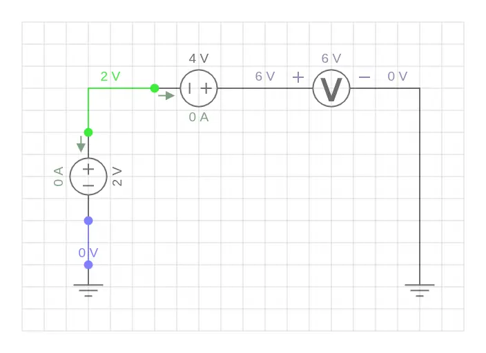
Why is there is no Current flow shown through the voltmeter?
Note: there is no Current flow shown through the voltmeter. This is because it is a perfect voltmeter, and as such has infinite impedance. Even so, it does measure the voltage potential!
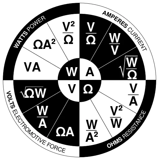
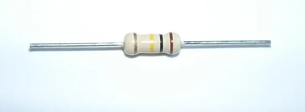
RESISTANCE AND OHMS LAW#
-
This is a picture of a normal axial Resistor with two leads.
-
This is normally used for through-hole PCB.
-
These may also be used for Ugly style, Dead bug style, Manhattan style or YooFab PCB style.
Resistance (R) of an electrical conductor is its opposition to the passage of Current. Resistance is measured in ohms (Ω). Electronic components that are designed to have a specific resistance. A Resistor maintains a constant relationship between the voltage across it (V) and the Current through it (I). This relationship is represented by Ohm's law:
\(I = V / R\)
Resistance and Ohms law

USEFUL FORMULA TRIANGLE#
-
It may be used to manipulate the \(I = V / R\) expression.
-
Put your finger over the term (I, V or R) that you need to evaluate.
-
Say we want to know the voltage, and we already know the resistance and the Current, then once your finger is over the V the triangle reads I | R
-
So, we then multiply \(I \times R = Voltage\)
-
Say we want to know how much Current is passing through a circuit, and we already know V and R. Put your finger over the 'I' symbol and the triangle tells you that the \(Current = V / R\)
LOST ENERGY IN ELECTRONS#
Electrons passing through a Resistor or any Conductor (No conductor is perfect) lose energy. The lost energy is dissipated as heat. If the Resistor cannot dissipate this energy as heat fast enough, it may then variously:
-
Explode with a loud bang!
-
Slowly burn, making nasty fumes.
-
Silently generate heat while all the time the constituent material used within the Resistor becomes putrescent due to this heat.
-
The whole Circuit Board may blow up.
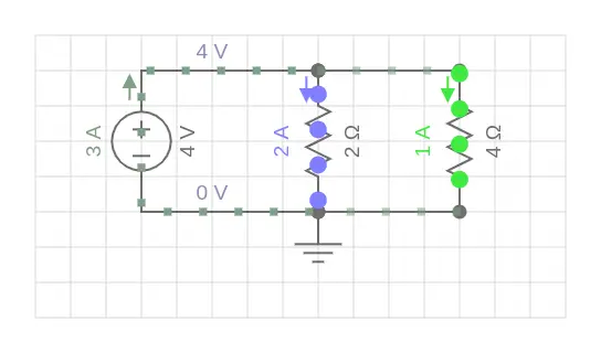
CONSTANT CURRENT & CONSTANT VOLTAGE#
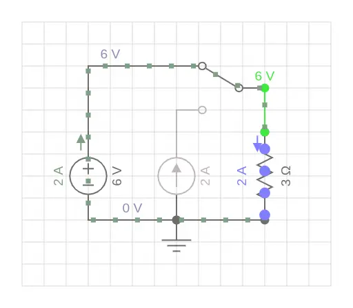
Above, the electric switch is flipped to apply a constant Voltage Source to the Resistor.
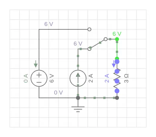
Now the Circuit connects a Constant Current Source to the Resistor.
The Current flowing in both examples is the same because in the top example we have 6V and an R of
Therefore, the
In the example below this, the constant Current source generates 2 Amps. So, the
KIRCHHOFF'S CURRENT LAW#
-
Kirchhoff's Current law (KCL) states that the sum of Currents flowing into a node is equal to the sum of Currents flowing out of that node.
-
KCL is based on the principle of charge conservation.
-
The simplest Current divider consists of two resistors connected in parallel.
-
It is important to remember that the same voltage exists across both resistors.
-
The input Current is divided such that less Current flows through the larger Resistor as it possesses stronger resistance.
THE CURRENT FLOWING#
TOTAL RESISTANCE OF ANY NUMBER OF RESISTORS IN PARALLEL#
To find the total resistance of all components, add the reciprocals of the resistances of each component and produce the reciprocal of the sum. The total resistance will always be less than the value of the smallest resistance:
In the above example, this is:
The current flowing through all parallel resistors may be calculated using Ohm's law:
KIRCHHOFF'S VOLTAGE LAW (KVL)#
-
Kirchhoff's voltage law (KVL) states that the sum of voltages across the components in any closed network loop is zero.
-
KVL is based on the principle of energy conservation.
-
The supposition is that the energy of an electron that makes a complete trip around the loop is unchanged.
The KVL Voltage divider
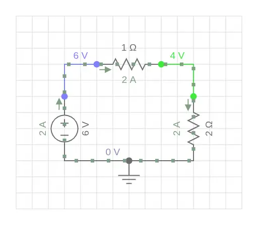
The simplest voltage divider is two resistors connected in series. Remember that the same amount of Electric Current flows through both resistors.
KVL for the three components in the loop: \(6Volts - 2Volts - 4Volts = 0Volts\). The voltage source “lifts” a positive charge up from the ground (energy supplied), then the charge “drops” back to the ground through the resistors (energy dissipated).
-
When Current flows through a larger value Resistor, it faces more resistance, which impedes more Current flow than when flowing through a smaller value Resistor.
-
Consequently, the input Voltage is divided such that the voltage drop (Voltage difference) across the larger value Resistor is bigger.
RESISTOR TREE#
The KVL Voltage divider
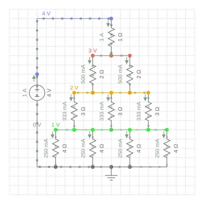
One way to calculate an equivalent resistance of a network is to apply a known voltage across it and then measure the Current drawn by the network. This example is intended to demonstrate resistors in Parallel & in Series at the same time.
RESISTOR TREE EVALUATION#
-
The equivalent resistance of this Resistor tree is \(4\Omega\) as it draws \(1 Amp\) of Current from a \(4 Volt\) source.
-
We see that, for each level, we have: \(N \times Resistors \times N \Omega\) which are connected in parallel; these are equivalent to \(1 \Omega\)
-
In this Circuit Schematic, each level of the tree acts as a \(1 \Omega Resistor\)
-
Therefore, the sum resistance of the tree from top to bottom is simply \(4 \times 1 \Omega Resistors\) in series, which is \(=4 \Omega\)
CAPACITOR (C)#
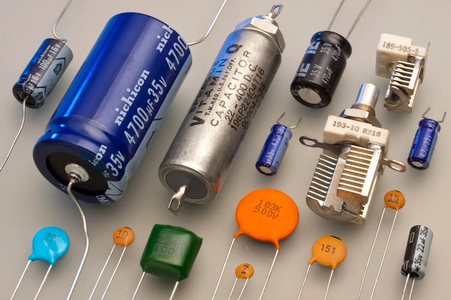
-
A Capacitor is a two-terminal component designed to store energy in an electric field. It consists of two isolated plates, such that no direct current can pass.
-
When an electron arrives at one plate, one electron leaves the other plate. As more electrons arrive, negative charge accumulates on one plate, and the same amount of positive charge accumulates on the other plate. Presence of positive charge means electron depletion.
Capacitor
Capacitance is denoted as C, and it is measured in Farads (F). Capacitance of one Farad storing a charge Q of 1 Coulomb at each plate causes a voltage V of 1 volt between the plates,
Constant current through a capacitor increases the charge at a constant rate, which, in turn, increases the voltage across the capacitor at a constant rate. Voltage is proportional to the integral of capacitor current, and the current is a time derivative of voltage.
RC STEP RESPONSE (RESISTOR - CAPACITOR STEP RESPONSE)#
RC step response
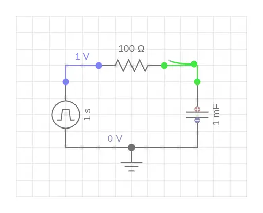
-
With a voltage step presented at the input, a Capacitor will charge. However, in this Circuit Schematic, we have a Resistor limiting the Current flow.
-
The time required to charge the capacitor to 63.2% of its full charge is known as The Time Constant:
- After five time constants, \(5 \times t\), the capacitor charge will reach 99.3%. But how do we calculate the time constant of the RC?
Thus,
We are interested in HALF pulse Duration, which is calculated:
Half of this duration:
A SQUARE WAVE#
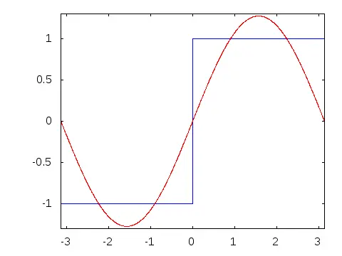
The above picture shows the Fourier series composition of a Squarewave, which is genuinely enchanting. However, here we are focused on the Reciprocal of the Frequency of our Squarewave. This is known as the Duration.
In this context, we are interested in each ± pulse (both positive going AND negative going).
In this example, the time duration we are interested in is HALF the Period as mentioned above.
INDUCTOR (L)#
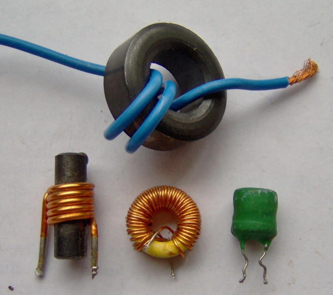
-
An inductor, also called a coil, choke, or reactor, is a passive two-terminal electrical component that stores energy in a magnetic field when electric current flows through it.
-
An inductor typically consists of an insulated wire wound into a coil.
-
When the current flowing through the coil changes, the time-varying magnetic field induces an electromotive force (e.m.f.) (voltage) in the conductor, which is described by Faraday's law of induction.
-
According to Lenz's law, the induced voltage has a polarity (direction) which opposes the change in current that created it.
-
As a result, inductors oppose any changes in current through them.
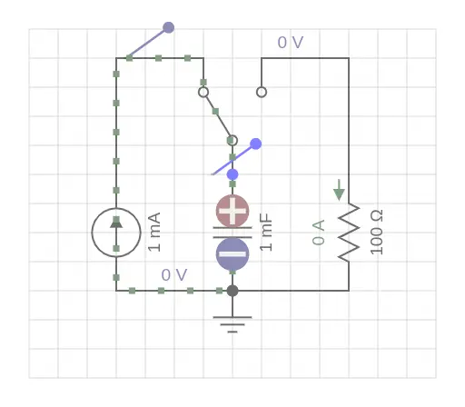
LC 'TANK' OSCILLATOR#
LC Oscillator
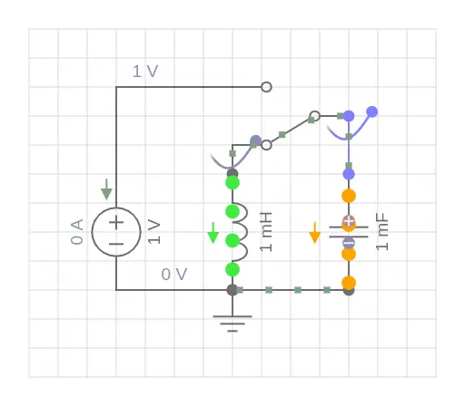
An LC circuit can store energy. An LC Circuit as pictured above is often known as a Tank.
-
At first, the charged Capacitor stores all the energy in its electric field.
-
Once the switch is flipped, the Capacitor starts to discharge through the Inductor.
-
The Current flow builds up a magnetic field around the Inductor until the Capacitor is discharged.
-
At this point, all the energy has been transferred to the Inductor and is stored in its magnetic field.
-
The Current subsequently flows in the opposing direction. This is because inductors oppose the change in Current.
-
The Capacitor is then charged with the opposite polarity until all the energy is transferred back to the Capacitor.
-
The energy keeps alternating between Inductor and Capacitor.
-
The Capacitor stores all the Circuit's energy when the Voltage is either at its positive or negative peak.
-
The Inductor stores all the Circuit's energy when Current is either at its positive or negative peak.
-
The Oscillation occurs with: \(\to Period = T = 2π√ L \times C\).
-
The Resonant Frequency is given by the Reciprocal of the: \(\to Period = Frequency = \frac {1} {T}\).
-
In this Circuit, the Inductor: \(\to L = 1 mH\)
-
The Capacitor: \(\to C = 1mF\)
-
\(\to Period = T = 2π√ L \times C \to T = 2π√1 mH \times 1mF = 6.28 mS\)
-
Resulting in an oscillation period: \(\to T = 6.28 mS\)
-
The Resonant Frequency: \(\to Frequency = \frac {1} {6.28 mS} = 159 Hz\).
-
This Circuit Schematic is built from 'idealist perfect' Component types that have NO losses. Thus, in this imaginary world, the Oscillation would continue forever.
-
However, in the real world, no Component is perfect, so the Oscillation would subside over a moderately short time.
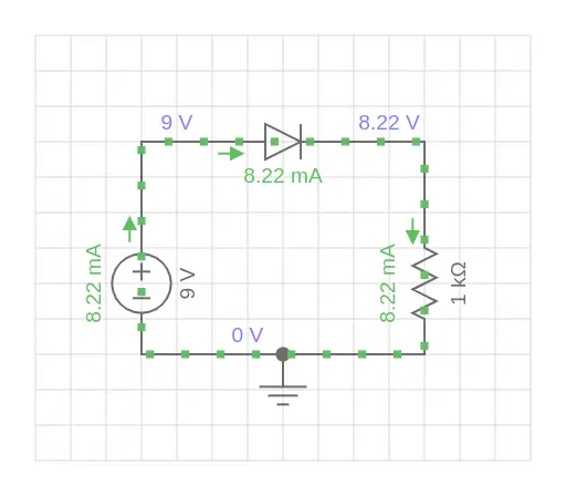
A DIODE#
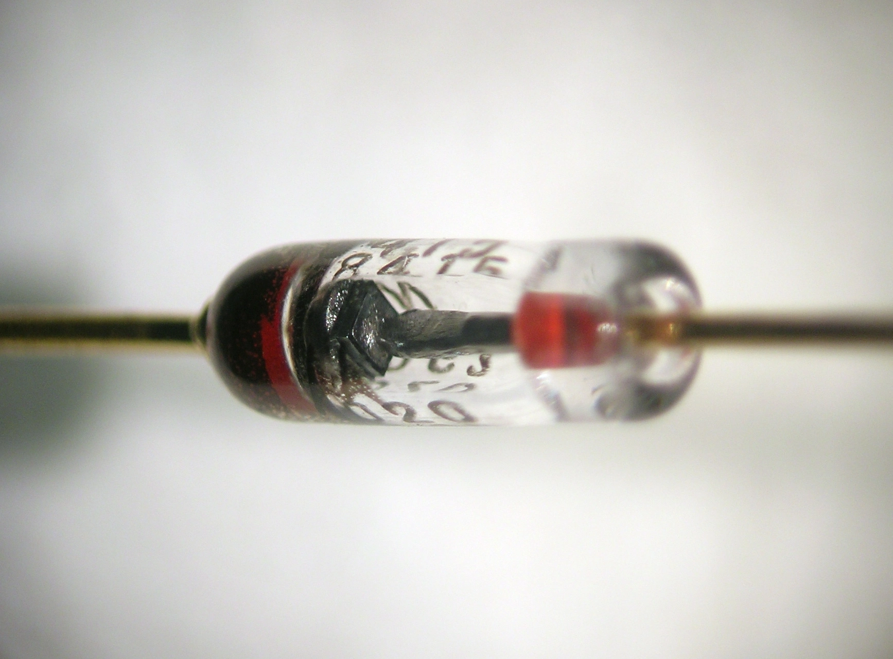
-
A Diode is a two-terminal component that has low resistance to Current flowing in one direction yet has high resistance to current in the opposite direction.
-
The Current flow is always from Anode to Cathode.
-
A silicon Diode starts to conduct Current when the forward voltage across it exceeds a threshold of about 0.6 V to 0.7 V.
Diode
DIFFERENT DIODES#
There are different diodes, in the sense that diodes may be constructed from various materials. The three most common diodes are:
- Silicon — Forward voltage drop 700 mV.
- Schottky — Forward voltage drop 400 mV.
- Germanium — Forward voltage drop 300 mV.
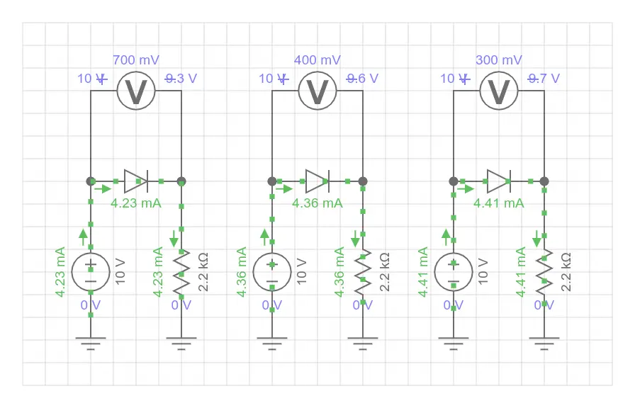
NOTE: PN diodes such as Silicon or Germanium always have a sightly differing voltage drop, depending upon the manufacturer, the batch and other factors.
Schottky Diodes are much more homogeneous. The main explanation for this is that these are formed by semiconductor to metal, rather than two types of differently doped semiconductor.
GENERAL INFORMATION ON DIODES#
As the forward voltage increases, the Current grows Exponentially.
You should never connect a Voltage source of over 1.5 V directly across a Diode, as there will be nothing to restrict the Current and this will damage the Diode.
A Current limiting Resistor should normally be connected in series with the Diode. Occasionally, the circuit at the Cathode side of the diode will suffice as the limiting resistor.
Diodes also play a role of a Protector. Assume that the Resistor in this Circuit Schematic, is a costly Gadget, this Diode then guards it from an empty-headed user inserting a Battery the wrong way around. (this user might be you, so don't pass judgement)
Reversed Diode
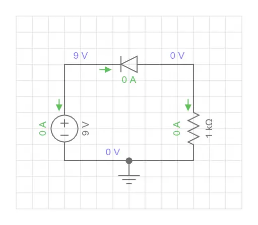
Note that in the above Circuit Schematic, the Diode does NOT conduct a current flow because the current is trying to go from Cathode to Anode, which will not work.
HALF WAVE RECTIFIER#
A half-wave rectifier Circuit Schematic
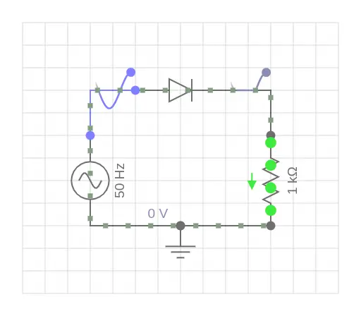
This shows half the AC voltage being rectified.
-
A rectifier is a circuit designed to convert alternating current to direct current. In a half-wave rectifier, the diode allows the current to flow only during the positive half of the AC wave. When the input voltage is negative, the diode blocks the current.
-
Although the resulting current is unidirectional, only half of the input AC wave reaches the output. This is not efficient, but occasionally, it is all that is needed.
FULL WAVE RECTIFIER#
A Full-wave rectifier Circuit Schematic
Note that this is one way of depicting a Bridge Rectifier.
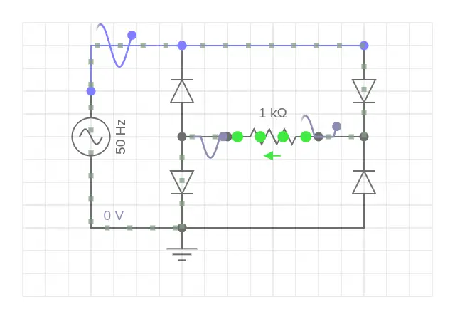
This Circuit Schematic shows all the AC voltage being rectified.
- A full-wave rectifier converts alternating current (AC) to direct current (DC). This diode bridge rectifier circuit is one implementation of a full-wave rectifier. Indeed, it is by far the most common method used.

The bridge rectifier is shown in the circuit above.
- During the positive part of the AC wave, only two of the four diodes let the current through the resistor (this represents the load or circuit)
- During the negative half-wave, the other two diodes allow the current to pass through the resistors. The current through the resistor is unidirectional, thanks to the configuration of the diodes.
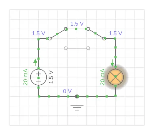
LED CURRENT LIMITING#
Limiting the Current supply to an LED at 20 mA
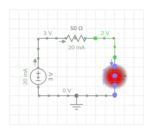
This Circuit Schematic shows a resistor used to limit the Current to 20 mA where we have a 3Volt Supply
-
When designing circuits with light-emitting diodes (LED), the risk is that too much current or voltage may damage the LED.
-
The simplest way to protect an LED is to include a current limiting resistor in series. LEDs have recommended operating voltage and current, based on which you can calculate the resistance using Kirchhoff's laws.
Limiting the Current supply to an LED at 1 mA
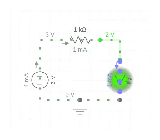
Due to the technological revolution in super bright LED indicators, the current needed to make an indicator perfectly visible on a panel has significantly lowered. Here, we only need 1 milliamp to power the LED, yet we use the same 3 Volt supply. This is much more efficient because it produces less heat.
Most of the colours are now available in Super Bright varieties, even though the above Circuit Schematic shows a green LED.
OPERATIONAL AMPLIFIERS#
DC INVERTING AMPLIFIER#
A DC inverting amplifier Circuit Schematic
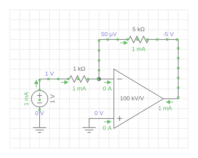
This Circuit Schematic inverts and scales the Direct Current input voltage. The gain of the inverting amplifier circuit is defined by the ratio of feedback and input resistors:
- In this case, the gain is negative, where A is the amplification factor.
- If the op-amp gain is high and the values are accurate, the circuit will be very accurate.
-
The 5 kilo-ohm resistor is connected between the output and the negative input of the op-amp. This creates negative feedback, which restricts the gain by feeding a proportion / ratio of the output voltage back to the inverting input. The input to the amp is grounded on the + input.
-
As mentioned above, the Ratio is determined by: \(Rfeedback / Rinput\).
-
This is called the closed loop gain. The closed loop gain of the inverting amplifier circuit is defined by feedback and input resistors:
DC NON INVERTING AMPLIFIER#
A DC non inverting amplifier Circuit Schematic
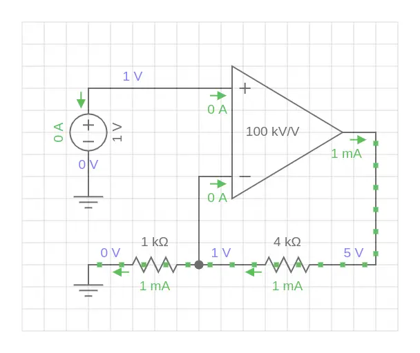
The gain of the non-inverting amplifier circuit is defined by the ratio of feedback and input resistors:
Where A = Amplification factor or Gain, where in this case the gain is positive.
-
As with the inverting amplifier, the gain of this circuit may be very accurate, so long as the op-amp gain is high, and the resistor values are accurate.
-
The 4KΩ resistor is connected between the output and the negative input of the op-amp. This creates negative feedback where a proportion / Ratio of the output voltage is fed back to the inverting input; thus restricting the gain.
-
The difference between the inverting amplifier and this Circuit Schematic, is mainly that the input voltage is presented to the + side of the op amp. Whereas, in the inverting amp, the input is passed through to the (negative) input side.
In this Circuit Schematic, the input impedance does NOT form part of the Gain equation, which is often useful as Operational Amplifiers often have very high Input Impedance.
BIPOLAR JUNCTION TRANSISTOR#

There are many packages used for bipolar junction transistors. The above diagram shows a number of these.
BJT devices principally deal with current
This means that a Load Resistor is needed to convert the current passing through the BJT into a voltage. It is the load resistor that creates the voltage difference.
INSIDE THE BJT#
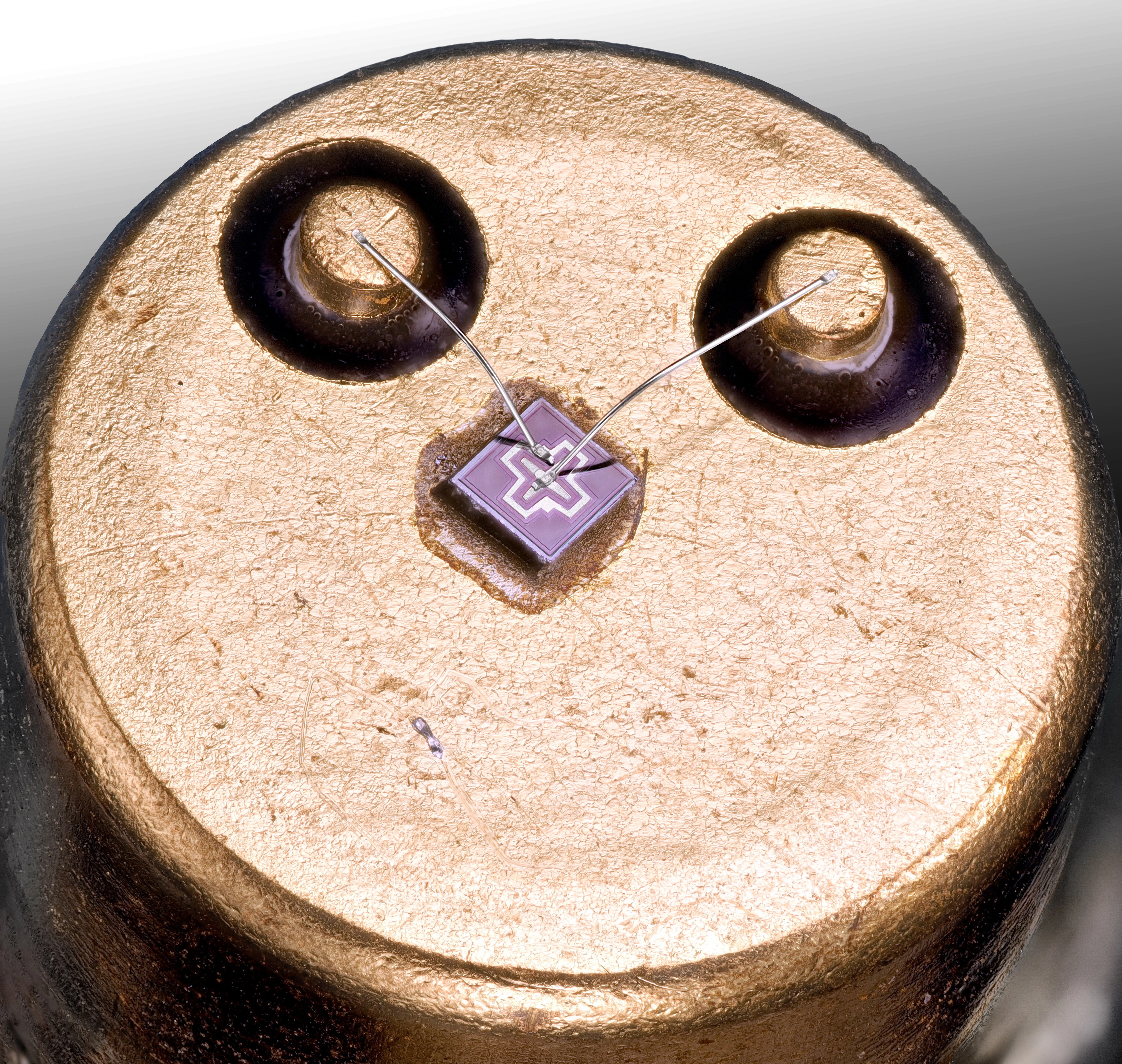
This is a photo of a MOTOROLA 2N2222 BJT.
This is what you might find inside a 2N2222 NPN transistor. In this case, the 'chip' of the transistor is connected to the outside via two leads and the body of the metal TO-18 package.
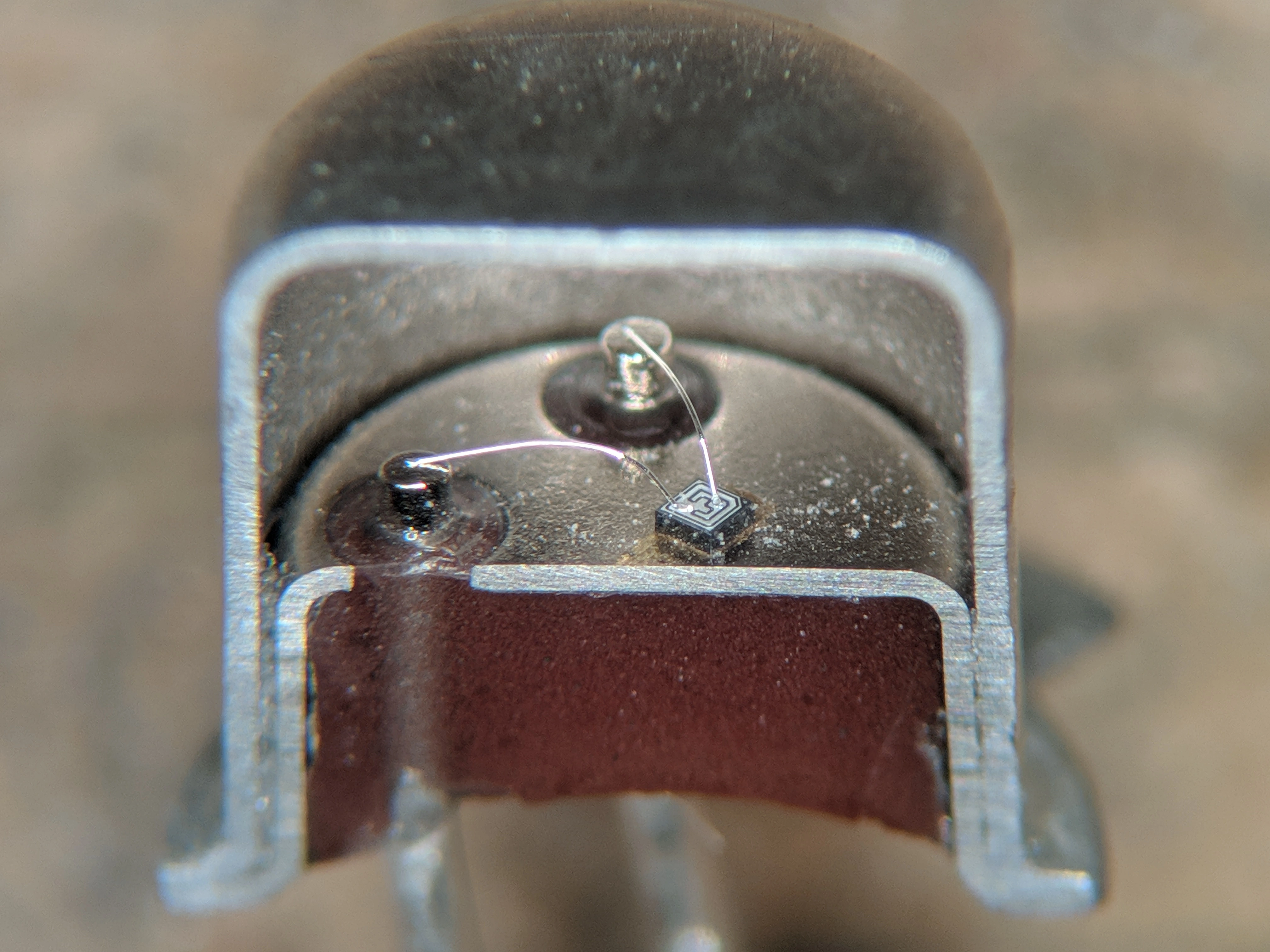
- This is a cross-section of another brand of 2N2222 transistors, also in the TO-18 metal package. The transistor is comparatively small when compared to its through hole package, as you can see. The manufacture of smaller Surface Mount versions of Semiconductor was spurred by this fact. The package used for SMD components is smaller than you might think. This helps achieve smaller and more cost-effective PCBs.
THE DOWNSIDE TO THIS MOVE TO SMD:#
- There are no actual leads in the sense of leads that can pass through a hole on a PCB, with only solder providing the mechanism for keeping the part on board. (This is not a massive problem as the mass of the device is less than the through hole one)
- SMD parts are small and often difficult to prototype with.
- The part is normally soldered onto the PCB using pick and place robots and then soldered using flow soldering methods. However, as these parts are now becoming prolific, widespread and often the only type of part you can buy, You may have to don your TRI-focal-goggles and use these (I have had to do this)
In essence, the shift toward Surface Mount Device (SMD) technology is primarily driven by profit. Sophisticated pick and place machines, essential for handling SMD components with precision, are typically beyond the reach of individual hobbyists and small-scale research and development firms. Interestingly, much like the emergence of the microprocessor revolution in 1978, the electronics industry has historically been propelled forward by grassroots innovators and enthusiasts. However, the adoption of SMD components by large corporations, driven solely by profit motives, poses challenges for these pioneers. This trend, evident since the industry's early days, has led to a slowdown in the rate of groundbreaking advancements for humanity.2
THE FUNCTION OF A BJT#
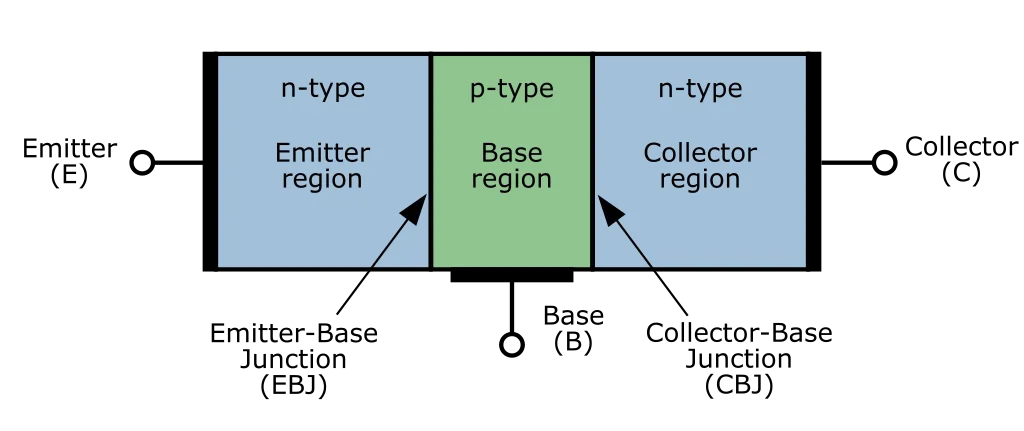
This is representative of the NPN BJT. It looks like two PN diodes as a sandwich. In other words, both the Collector — Base & the Emitter — Base junctions act as diodes, and can be used as such if, and only when, just two terminals are used.
WHAT CAN WE DO WITH A BJT?#
-
A BJT may be used as a switch (in its non-linear mode)
-
BJTs may also be used as Amplifiers.
-
A BJT may be used as a buffer.
Designing with a BJT, requires some thought about its intended function within a circuit. Unlike the Operational Amplifier above, the formulae for amplification is not quite as simple. However, neither is it so complex to cause a major Mental breakdown nor a total brain failure for the Designer.
Indeed, we tend to use established configurations of BJT Circuitry, which is a good thing because these are well-tried and tested.
Operating Modes of BJT Transistors
Depending on the biasing conditions like forward or reverse, transistors have three major modes of operation, namely:
ANY TRANSISTOR PN JUNCTION WILL ACT AS A DIODE.#
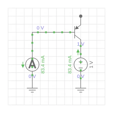
The above shows a PNP Transistor with Current passing from the Collector to the Base. The table below shows all combinations of these PN junctions within both NPN and PNP BJT(s).
TABLE SHOWING BJT MODES OF OPERATION#
| Junction type | Applied voltages | Junction bias | Mode | Active Linear |
|---|---|---|---|---|
| PN of NPN | ||||
| B>E | B>E | Forward | Diode | |
| E>B | E>B | Reverse | Diode | |
| B>C | B>C | Forward | Diode | |
| C>B | C>B | Reverse | Diode | |
| NPN | ||||
| E < B < C | Forward | Reverse | Forward-active | ✅ |
| E < B > C | Forward | Forward | Saturation | |
| E > B < C | Reverse | Reverse | Cut-off | |
| E > B > C | Reverse | Forward | Reverse-active | ✅ |
| PN of PNP | ||||
| B>E | B>E | Reverse | Diode | |
| E>B | E>B | Forward | Diode | |
| B>C | B>C | Reverse | Diode | |
| C>B | C>B | Forward | Diode | |
| PNP | ||||
| E < B < C | Reverse | Forward | Reverse-active | ✅ |
| E < B > C | Reverse | Reverse | Cut-off | |
| E > B < C | Forward | Forward | Saturation | |
| E > B > C | Forward | Reverse | Forward-active | ✅ |
CUTOFF MODE#
Cutoff Mode
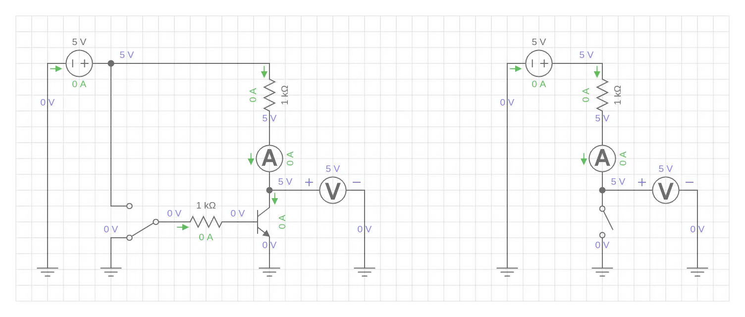
On the left-hand side there is a Circuit showing an NPN BJT used in Cutoff Mode. To the right of this is a simplified circuit equivalent. Here, we replace the BJT with a switch.
In this mode, both collector base junction and emitter base junction are reverse biased. As both the PN Junctions are reverse biased, there is almost no current flow except small leakage currents (usually in the order of few nano amps or pico amps).
The BJT in this mode is switched OFF and is essentially an open circuit.
What is the result of the 'Switch' being OFF?
Here, it is important to remember that because the BJT or Switch is OFF, this results in the supply voltage available at the output.
SATURATION MODE#
Saturation Mode
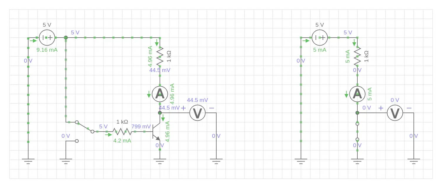
In this mode of operation, both the emitter-base and collector-base junctions are forward biased. Current flows freely from collector to emitter with almost zero resistance. In this mode, the transistor is fully switched ON and is essentially a closed circuit.
What is the result of the 'Switch' being ON?
Here, it is important to remember that because the BJT or Switch is ON, this results in almost ALL the supply being ditched to ground. Thus, the output of the Circuit is near the ground level
Used for digital and switching
Both Cutoff & Saturation modes are used for switching and digital logic circuits or switching on and off a relay/ solenoid
ACTIVE MODE — BJT AMPLIFIERS#
The three main BJT amplifier topologies are:
COMMON EMITTER AMPLIFIER#
Common emitter
About the Common emitter amplifier
A common-emitter amplifier is one of three basic single-stage bipolar-junction-transistor (BJT) amplifier topologies, typically used as a voltage amplifier. It offers high current gain (typically 200), medium input resistance and a high output resistance. The output of a common emitter amplifier is 180 degrees out of phase to the input signal.
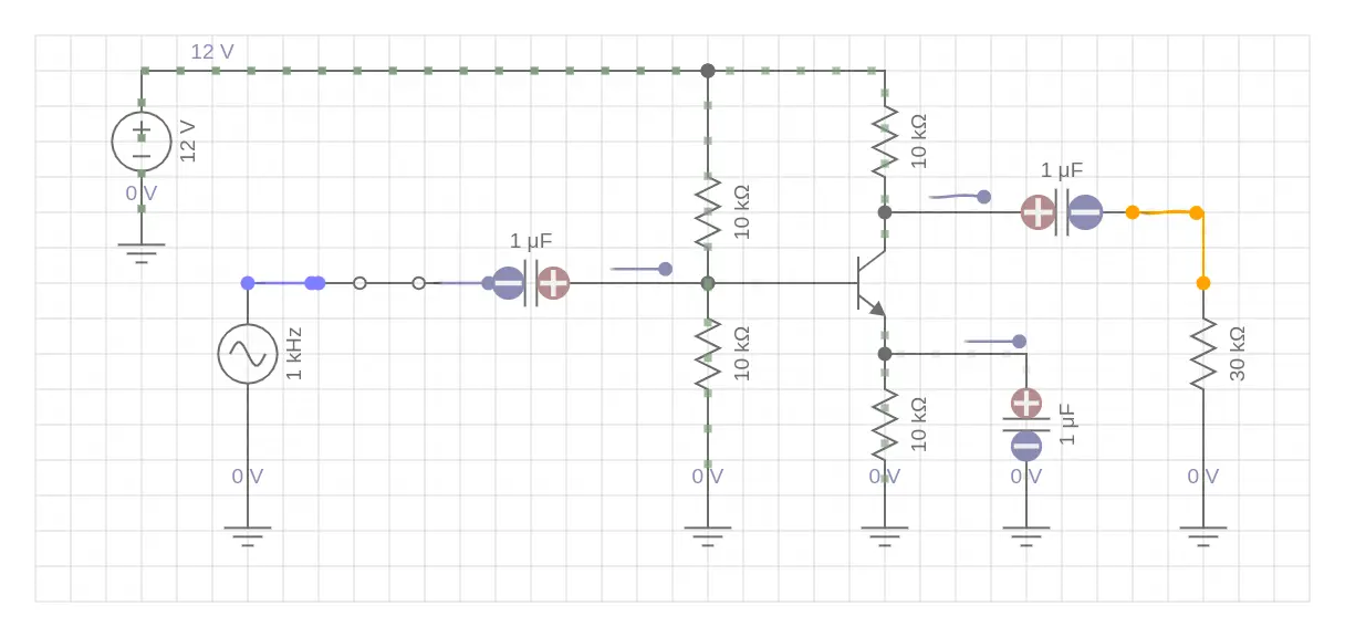
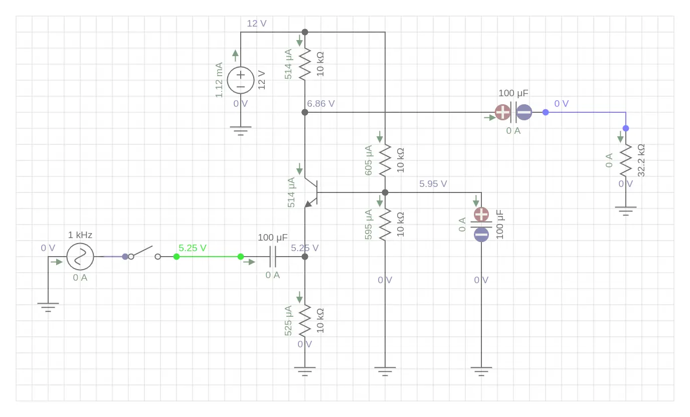
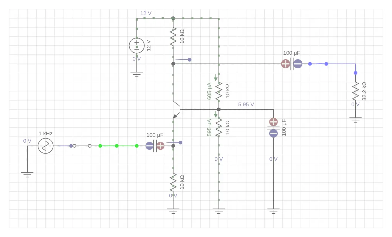
Common emitter with simple biasing & no signal
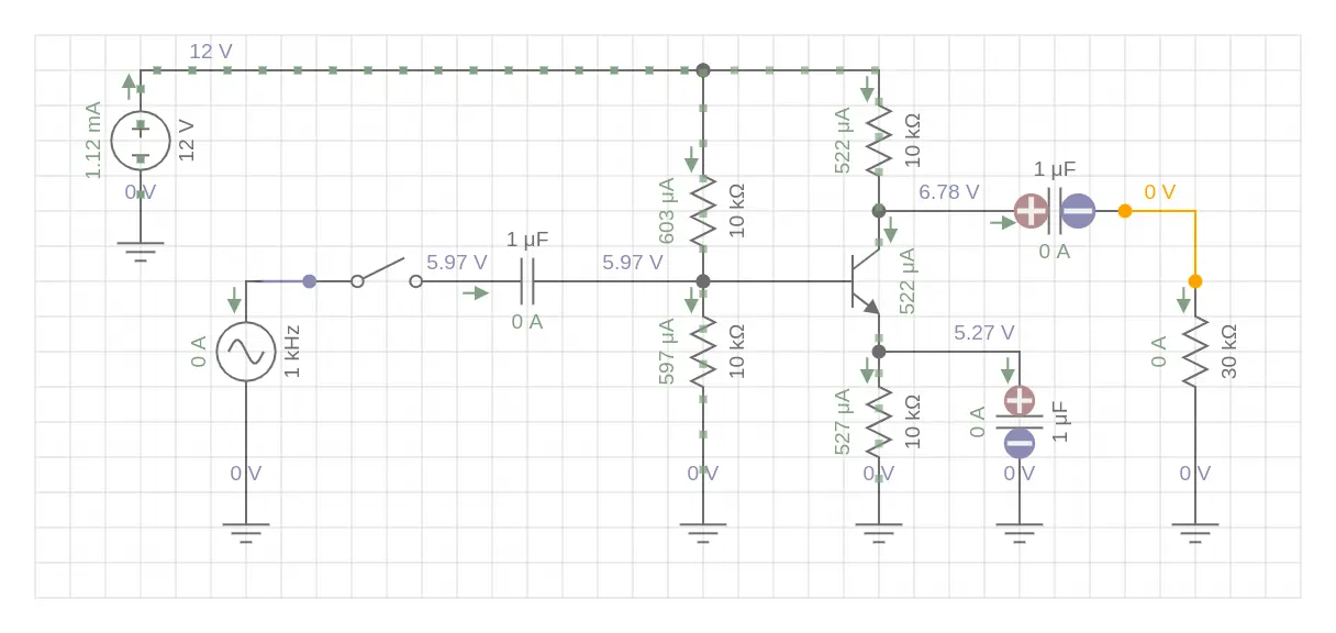
This shows the biasing, which uses 10K ohm resistors in all locations. Here we see the Common emitter amplifier with no signal input. This is interesting, as then we can note the current and voltages.
As you can see, the Base of the NPN BJT, is biased at around half the supply voltage. There is about a 1.5 Volt drop across the Collector to Emitter. The Quiescent current drawn, with no signal, is about 1 milliamp.
The circuit does have a bypass capacitor on the Emitter degradation Resistor. Here, as there is no signal, this will have no effect.
Common emitter with simple biasing with 10 mV p-p input
Here we see the same amplifier with a 10 mV p-p input signal. At the output, there is a 436 mV signal.
- 7.06 mV RMS input
- 311 mV RMS output
Common emitter with simple biasing with 10 mV p-p input, No bypass capacitor
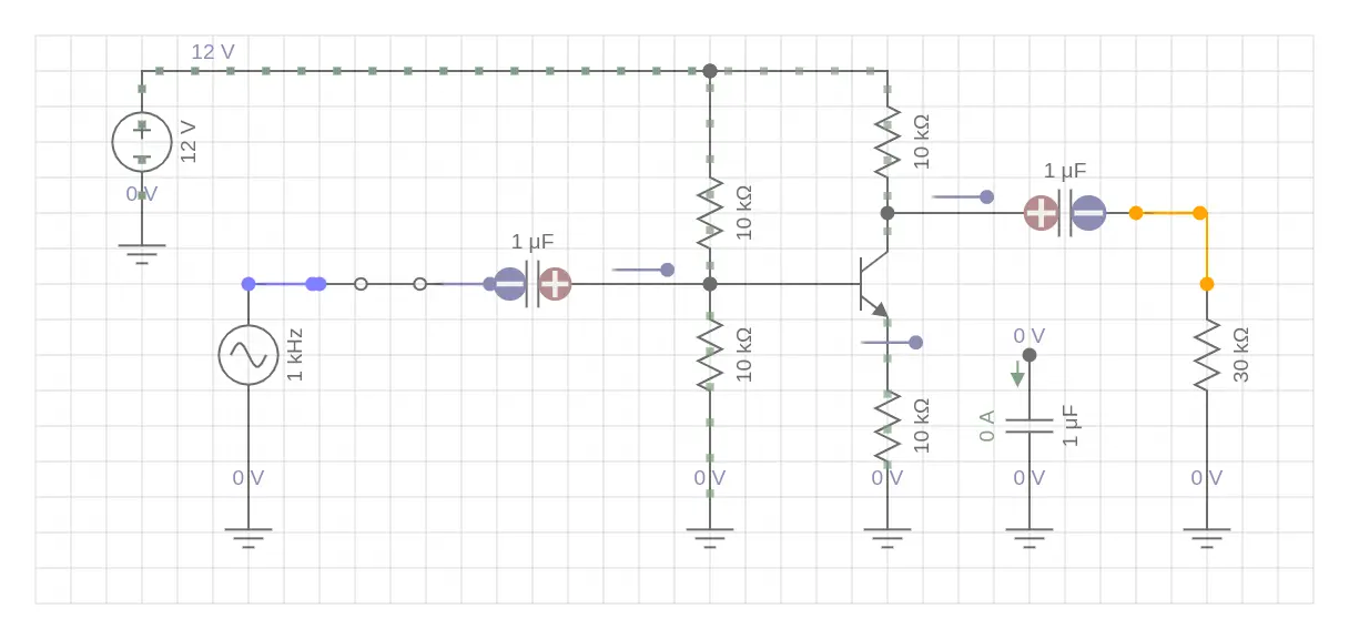
This is fascinating, as it is the same circuit, but the bypass Capacitor has been removed.
Result:
- 7.06 mV RMS input
- 5.22 mV RMS output
So, without the bypass Capacitor, this is no longer an Amplifier.
COMMON BASE AMPLIFIER#
A common-base (also known as grounded-base) amplifier is one of three basic single-stage bipolar junction transistor (BJT) amplifier topologies, typically used as a current buffer or voltage amplifier. In this circuit, the emitter terminal of the transistor serves as the input, the collector as the output, and the base is connected to ground, or “common”, hence its name.
It features very low input impedance, which is useful in RF applications. It's also used in some audio applications, where it is usually employed for amplifiers that require an unusually low input impedance, for example to act as a preamplifier for moving-coil microphones.
It is common within integrated circuits and in high-frequency amplifiers. For example, for some HF, VHF, and UHF because its input capacitance does not suffer from the Miller effect, which degrades the bandwidth of the common-emitter configuration.
It also has a high isolation between the input and output. This high isolation is useful in many RF applications.
Common Base Amplifier with simple biasing with NO signal input
Here we see a Common Base Amplifier, with simple biasing. Note that the Base is DC biased to midrail, yet at AC, it is grounded.
Also in this diagram the signal is not connected, so we can observe the current and voltages within the Circuit.
Again, the Quiescent Current is about 1 Milliamp.
Common Base Amplifier with simple biasing with a 1 mV signal input
Here we see the same Common Base Amplifier circuit, with a very low signal of 1 mV RMS presented to the input.
Result:
- 1 mV RMS input
- 148 mV RMS output
COMMON COLLECTOR OR EMITTER FOLLOWER AMPLIFIER#
In electronics, a common collector amplifier (commonly known as an emitter follower) is one of three basic single-stage bipolar junction transistor (BJT) amplifier topologies, typically used as a voltage buffer. Importantly, the output is in phase with the input.
The base terminal of the transistor serves as the input, the emitter is the output, and the collector is common to both (for example, it may be tied to ground reference or a power supply rail), hence its name.
The analogous field-effect transistor circuit is the common drain amplifier and the analogous tube circuit is the cathode follower.
It never saturates, even when the input voltage reaches just under HALF the positive rail.
The Emitter follower may have a very high input impedance, which means that it will amplify signals with very feeble current. Here when we say 'amplify', there is typically no voltage gain, and so the output is a copy of the input but buffered to provide a bolstered current.
It also provides a certain immunity to the previous stage. In other words, the buffering allows the next stage on from the buffer NOT to affect the preceding stage. (the stage before the Emitter follower.)
Emitter follower Amplifier without input signal
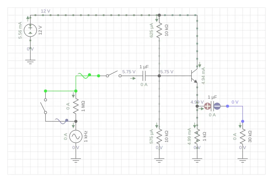
Here we see an Emitter follower Amplifier, with simple biasing. Note that the Base is DC biased to midrail. The base is also the input to this amplifier.
Here the load Resistor is just under the Emitter. We have set this to 1K ohms such that the amplifier may provide a higher current than in the previous cases, where the load Resistor was set at 10K ohms.
Also in this diagram the signal is not connected, so we can observe the current and voltages within the Circuit.
The Quiescent Current is about 5.5 Milliamps.
Emitter follower Amplifier with input signal
Here we see the same Emitter follower Amplifier, with a signal of 3V RMS presented to the input.
Result:
- 3V RMS input
- 3V RMS output
Emitter follower Amplifier with a high Impedance input signal
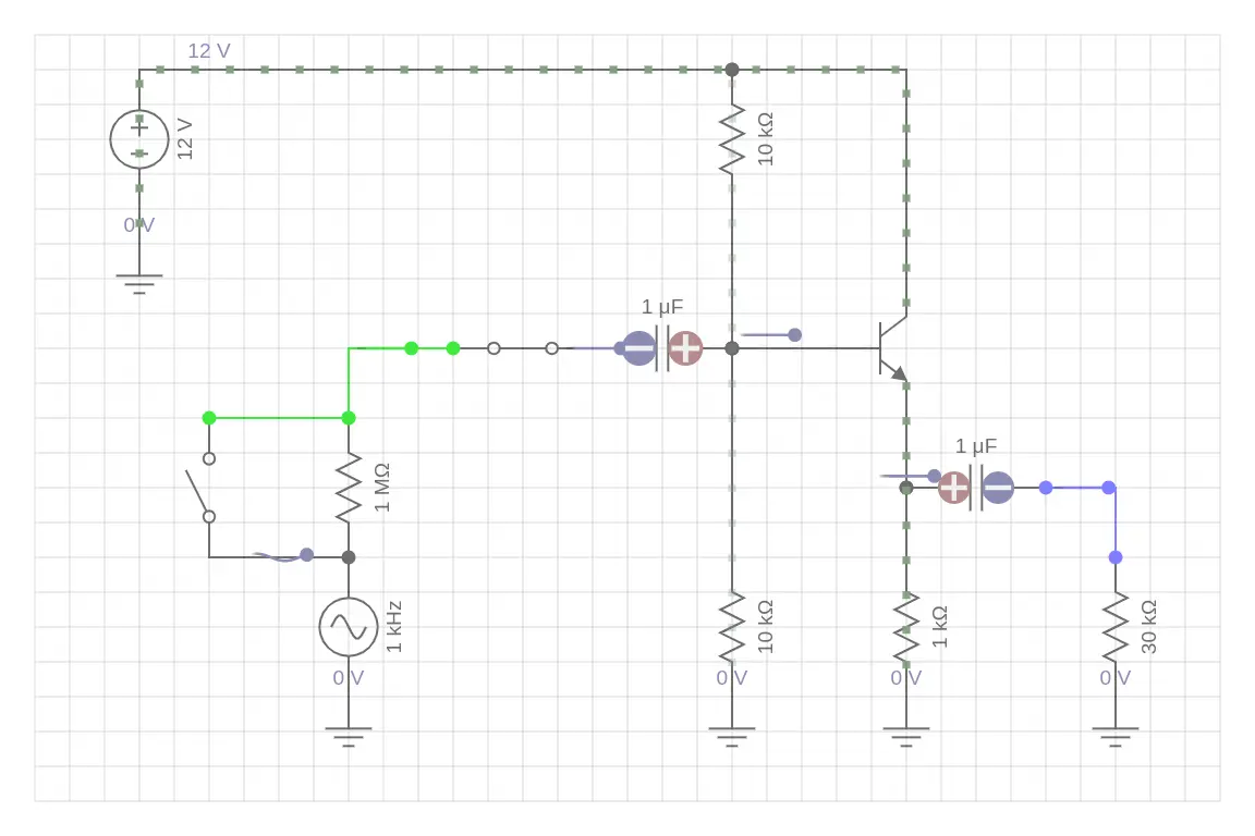
Here we see the same Emitter follower Amplifier, with a signal of 5 mV RMS presented to the input. This is measured after the 1 M ohm resistor. The signal generator is set at 1.5 Volts p-p.
Result:
- 5 mV RMS input
- 5 mV RMS output
FOOTNOTES#
-
The convention of Current flow is from Positive to Negative. However, when we mention Coulomb(s) we are specifically referencing Electrons. As these have a Negative charge, in the context of Coulomb(s), we revert to thinking in terms of flow from Negative to Positive. Immediately after this, we resume the Positive to Negative convention and pretend that we had not even mentioned Coulomb(s). ↩
-
Such comments as these reflect the opinion of Geoff. Others, may not resonate with his opinion. However, he does not really care if you do not agree with him; you can do a dance, jump up and down in muddy puddles, or get eaten by cardboard cutout crocodiles. ↩